


Second in a Series of 3
In Part 1 I talked about how making a device smaller isn’t always a good thing. This week I want to talk about how the push to use smaller packaging can be counterproductive.
To be fair, most of the innovation in electronics is in making devices smaller. Making devices smaller increases speed, reduces power consumption, and allows product designers to pack more functionality in without making their products bigger. For example, the evolution of switching devices from early thermionic valves (vacuum tubes, ~0.000277 switches per mm²) to modern FinFETs (~100 million switches per mm²) has put smartphones into our pockets with roughly 1 billion times the processing power of the room-sized ENIAC computer from 70 years ago. The evolution of electronic packages, from hollow glass tubes in the 1940s to today’s wafer-level chip-scale packaging, also played a big role in achieving this incredible level of miniaturization.
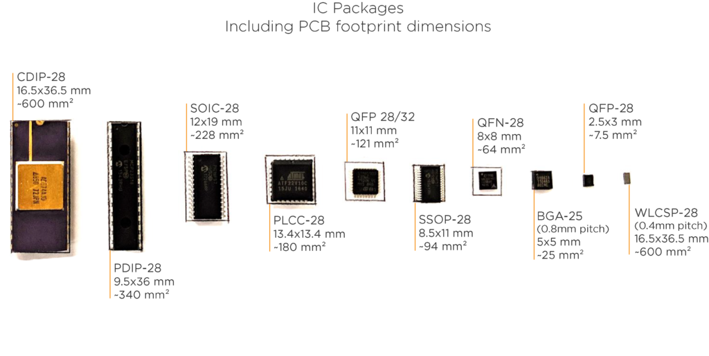
Reducing the package size does reduce the overall solution size when the package size is the limiting factor. This is often true of very simple digital ICs, such as combinatorial logic or small microcontrollers. For example, the transition from DIP to SOIC packaging of standard logic families had a dramatic effect on the size of computers for two main reasons:
- The ICs in a DIP package were never the same long thin shape as the package, so a significant amount of wasted space was reclaimed by cutting the pin pitch, and therefore the package length, in half
- The elimination of the through-hole for the pins dramatically improved routing density, particularly with high layer count PCBs, and improved component density by freeing up the backside of the PCB for component placement
Unfortunately, even with small digital ICs, there are diminishing gains with package reduction as it trends towards the obvious limit: the die size. The state of the art for high-density packaging is wafer-level chip scale packaging, which is accomplished by designing the pads into the die masks (or on a thin polyimide routing layer) and passivating the bare die. The “package” in this case is a passivation layer, often Silicon Nitride or an organic film, that may be only 1-2µm thick. Reducing the package to less than a few microns of film will have no meaningful effect on the overall size of the component, so WLCSP is a practical limit for package density. Further gains can only be achieved by reducing die size, not the packaging.
While reducing package size can work well for small digital ICs, it rarely works for power electronics, RF, analog signal conditioning, filters, or other electronics that depend upon physical characteristics that are not scaled with the IC package.
For example, an RF IC like the Nordic nRF52832 is available in a 6x6mm QFN and a 3.0×3.2mm WLCSP. Migrating from the QFN to the WLCSP reduces package size by over 25mm², a 75% reduction; however, the total Bluetooth solution also includes two external quartz crystals, an RF matching network, and a 2.45GHz antenna, totaling over 500mm². Reducing the package size reduces the solution by 5% or less. The solution size may not decrease at all because of layout constraints on the crystals and the antenna. By focusing on antenna design rather than the IC we’ve achieved a much more dramatic solution size reduction of 60%.
For power electronics, the dependence upon external components or features can be easily seen by plugging almost any numbers into TI’s Webench software. The default input values, 2A at 3.3V, resulted in a range of regulator solutions with different IC packages. Two of the first results (at the time this was written) are the TPS5429 and the LM3485. Both solutions have roughly the same input, output, and efficiency characteristics.
| Regulator IC | Package Size | # External Components | Solution Size |
| TPS5429 | 5x6mm (30mm²) | 14 | 232mm² |
| LM3485 | 3x5mm (15mm²) | 12 | 560mm² |
The LM3485 has half the package size but results in more than twice the solution size. In this case, the solution size is dominated by the external inductor and capacitors. The higher switching frequency of the TPS5429 allows for smaller external inductors and capacitors, resulting in a much more significant effect on solution size than the smaller IC package size.
Reducing the size of external components, such as the antenna or the external inductor, is an effective tool to achieve modest solution size reduction. For substantial solution size reduction, the key is to eliminate external components entirely and integrate their functionality into highly integrated ICs. Decades ago, control systems used small microprocessors with an external program and data memory, and a small set of peripherals. Over the past 25 years, the memories were integrated into the microcontroller IC and the peripheral sets grew to include dozens of communications protocols, autonomous event-driven peripheral interconnects, and integration of advanced analog front-end functionality. Modern microcontrollers provide single-chip solutions to products that five years ago would have required external op-amps, external precision ADCs and DACs, and an FPGA for servo motor control.
While it may sound simple to remove components and integrate their functionality into a single-chip solution, the unfortunate truth is that highly integrated microcontrollers offer much less design flexibility than discrete solutions. For example, integrated peripherals perform differently than their discrete counterparts. The entire system design must be tailored to work with the peripherals available in the selected microcontroller family, often requiring creative circuit design and a deep understanding of how to trade performance for integration. At Sunrise, we have a team of expert electronics designers and systems engineers who regularly tackle these sorts of design challenges. But that’s another topic for another blog post.
Check Out Misconceptions of Miniaturization: Part 3
FAQ’s
1. Why do people think smaller packaging automatically means a smaller solution?
There are two main reasons:
- People associate smaller components with smaller devices.
- In some cases, reducing the package size of an integrated circuit (IC) can significantly reduce the size of the finished product.
2. What are the limitations of reducing package size?
- There are diminishing returns as the package size approaches the size of the die itself.
- Other components, such as crystals, antennas, and inductors, may limit the overall size reduction of a device.
3. When does reducing package size make sense?
Reducing package size can be effective for small digital ICs, such as logic families or microcontrollers.
4. When does reducing package size not make sense?
Reducing package size is not as effective for:
- Power electronics
- RF electronics
- Analog signal conditioning
- Filters
- Other electronics that depend on physical characteristics
5. What are some alternative ways to achieve miniaturization?
- Reduce the size of external components, such as antennas and inductors.
- Integrate the functionality of external components into highly integrated ICs.
6. What are the challenges of using highly integrated ICs?
- They offer less design flexibility than discrete solutions.
- The system design must be tailored to the specific peripherals available in the microcontroller family.